


Semiconductor
VIA wafer depth measurement
Date:2020-06-04
Source:Samsun Technology
VIA wafer depth measurement using white light spectral interferometric sensors

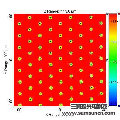
Wafer depth measurement 3D profile
Depth measurement 2D topography

Depth = 112.3 +/-0.4 μm

Depth = 65.28 +/- 0.1 μm

Depth = 87.28 +/- 0.6 μm
